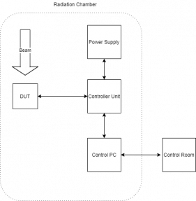
Mass memory systems for space applications require suitable density to be able to store the high amount of the data generated by satellites and space probes. Currently there are no High-Reliability devices that can compete with commercial flash devices in terms of costs, memory density, power and device size. However, since the mass memory is typically critical for the mission success (subsystem criticality category Q0), the use of the commercial high-density memory devices conflicts with reliability, availability and radiation tolerance requirements. From the high potential that commercial memory devices have compared to Hi-Rel devices and the criticality category of a mass memory system, results the need for further screening, qualification and radiation testing activities. This need is additionally amplified by the short lifespan of commercial devices compared to Hi-Rel devices. NAND flash devices provide a high-density non-volatile solution for mass storage application. Single-level Cell Flash technologies down to a feature size of 25nm are already used for spaceborne mass storage applications. However, the reduced feature size increases the single event effect (SEE) sensitivity since only a reduced amount of charge is stored in the floating gate of the cell. Instead, novel 3-dimensional approaches of several stacked active layers of less demanding feature size are of high interest and are also currently evolving to the major technology on the market. With the larger feature size, a lower SEE sensitivity is expected, as it was for previous generations of planar devices, but still providing a significantly higher storage density. First radiation test campaigns of 3D devices lack the characterization of the peripheral circuitry to give a full view on the feasibility for the use in the space environment. This gap shall be closed and results of this characterization shall give inputs to the predevelopment of future mass memory systems.

