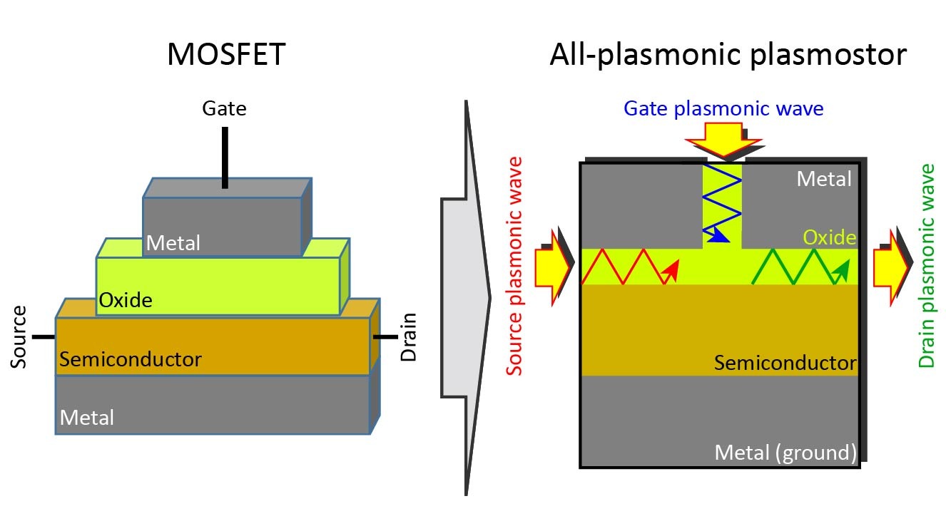
The design of electric circuits for the Space environment requires special attention due to a number of potentially risky scenarios, as energetic particles can cause a wide variety of issues, ranging from temporary data corruption to permanent damage. Space applications require new approaches and even new technologies. In this regard, we shall extend the concept of MOSFET (Metal Oxide Semiconductor Field Effect Transistor) towards the field of photonics by introducing a special kind of optical transistor, known as plasmostor – PLASmonic Metal Oxide SemiconducTOR - whose working principle relies on the generation and control of surface plasmon polaritons. The plasmostor will be digitally realized within a multiphysics framework, hence allowing its in-deep analysis and comprehension which will lead to an exact plasmostor behavioral prediction without the need for actual field testing.
This digital twin philosophy will also grant the possibility of pursuing plasmostor designs compatible with the fabrication requirements of nowadays microelectronics foundries, therefore paving the way for its actual experimental implementation. Furthermore, simulation testing will be performed for different Space-related scenarios, from orbiting satellites to close-to-Sun missions, including on-land situations such as Moon or Mars rovers.
The final objective is to implement a powerful numerical tool capable of leading to the design of an optical transistor resilient to ionizing radiation in the Space environment.

